


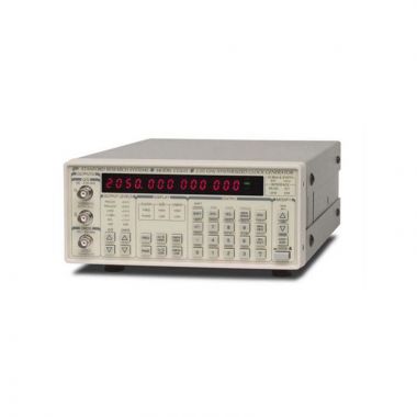
SRS CG792 Multichannel Clock Generator

- Clocks from 1 mHz to 2.2 GHz
- Up to four synchronizable outputs
- Random jitter less than 1 ps rms
- 11 digits of frequency resolution
- 100 ps rise and fall times
- Frequency and phase modulation
- OCXO and rubidium timebase (opt.)
- USB, Ethernet, and RS-232 interfaces
Lambda Exclusive Promotion:
Additional 12 months warranty for free (2 years total) via our UK Service Centre.
The Stanford Research Systems CG635 generates extremely stable square wave clocks between 1 µHz and 2.05 GHz. The instrument's high frequency resolution, low jitter, fast transition times, and flexible output levels make it ideal for use in the development and testing of virtually any digital component, system or network.
The SRS CG792 extends precision clock synthesis capabilities with up to four independent ultra-low jitter outputs from 1 mHz to 2.2 GHz. Reliable, low-jitter clocks help maintain signal integrity in systems using high-speed ADCs and DACs and other applications, minimising artifacts caused by jitter and modulation.
In communications systems and networks, jitter, wander, or frequency offsets can lead to high bit error rates or total loss of synchronization. The CG792 provides exceptionally clean, stable clocks required for the most critical applications while setting new standards for frequency accuracy, phase noise performance, and operational flexibility.
The CG792 extends precision clock synthesis capabilities with up to four independent ultra-low jitter outputs from 1 mHz to 2.2 GHz. Reliable, low-jitter clocks help maintain signal integrity in systems using high-speed ADCs and DACs and other applications, minimizing artifacts caused by jitter and modulation.
Advanced New Architecture
At the heart of the CG792 lies a sophisticated dual analog PLL architecture utilizing state-of-the-art reference synthesizer phase locked loops. This design employs intelligent spur avoidance algorithms that automatically select optimal reference frequencies to eliminate integer boundary spurs. The system automatically chooses between several precision reference frequencies to maximize phase detector frequency while minimizing spurious content, maintaining decimal frequency resolution with seamless frequency transitions.
Precision Timebase Options
The CG792 accommodates diverse timing requirements with multiple timebase configurations. The standard crystal timebase provides excellent stability, while optional OCXO or rubidium frequency standards offer higher precision for demanding measurements. An external 10 MHz reference input with automatic detection ensures compatibility with existing laboratory standards.
Versatile Outputs
Each channel provides three synchronized outputs optimized for different applications. High-speed differential outputs provide square waves with programmable offset and amplitude and sub-100-picosecond transition times. The CMOS output delivers fixed 3.3 V logic levels optimized for high-impedance loads.
Low Phase Noise and Jitter
With exceptionally low phase noise and high frequency resolution, the CG792 can replace RF signal generators in many applications. Front-panel outputs provide square waves up to +7 dBm — ideal for driving RF mixers.
Advanced Phase Control and Synchronization
The CG792's built-in phase measurement system enables automatic channel synchronization. Hardware-based channel coupling establishes deterministic phase relationships, while fast phase slew enables rapid timing adjustments.
Comprehensive Modulation Capabilities
The built-in modulation system supports both phase and frequency modulation using a range of standard built-in waveforms as well as a user-applied analog signal via the rear-panel BNC input. In Jitter mode, the clock edges can be modulated with up to 3 ms of jitter. Additional capabilities include output blanking, polarity inversion, and pseudo-random bit sequence generation.
Intuitive Touchscreen Interface
The CG792 features a 5-inch colour TFT display with capacitive touch interface. The system organizes functions through intuitive tabs covering clocks, keypad entry, synchronization, modulation, and settings. Large numeric readouts combine with comprehensive parameter tables for immediate visual feedback.
Universal Connectivity
Standard Ethernet connectivity supports DHCP and static IP configuration, while USB and RS-232 interfaces provide flexible connection options. Command language based on SCPI ensures straightforward integration into automated test systems with IEEE 488.2 common command support.
Environmental Stability and Reliability
Designed for long-term laboratory and production use, the CG792 incorporates temperature-compensated control systems that minimize drift over varying operating conditions. Robust shielding and optimized PCB layout reduce susceptibility to crosstalk and electromagnetic interference, ensuring consistent performance even in electrically noisy environments.
Applications
Digital Circuit Development: Provide stable clock references for FPGA, microprocessor, and ASIC testing with precise frequency and phase control.
Communications Testing: Generate complex clocking scenarios for network equipment validation, including multi-rate testing and protocol compliance verification.
Instrumentation Synchronization: Serve as a master timebase for test systems requiring multiple synchronized frequencies with deterministic phase relationships.
Precision Measurements: Support high-resolution timing measurements with ultra-low jitter reference signals and programmable modulation capabilities.
| Frequency | |
| Range | DC, 1 mHz to 2.2 GHz |
| Resolution | 11 digits |
| Settling time | <1 s (0.25 s above 100 Hz (typ.)) |
| Phase | |
| Range | ±360 °C |
| Resolution | |
| f < 200 Hz | Δφ ≤ 30 µdeg. × f |
| f ≥ 200 Hz | Δφ ≤ 0.01 µdeg. × f |
| Setting time | <2.0 s + 2/f (typ.) |
| Sync accuracy | <250 ps |
| Sync repeatability | <25 ps |
| Sync time | 3 s + 2/f (typ.) |
| Differential Outputs | |
| Outputs | BNC |
| Frequency range | 1 mHz to 2.2 GHz |
| Common mode | -3.0 V to + 2.0 V |
| Amplitude (p-p) | 0 V to 1.2 V |
| Level resolution | 25 mV |
| Level error | < 1.5 % ± 25 mV |
| Transition time | <100 ps (20 % to 80 %) |
| Asymmetry | <100 ps from nominal 50 % |
| Source impedance | 50 Ω (± 1 %) |
| Load impedance | 50 Ω to ground on both outputs |
| Polarity inversion | Rear-panel BNC input |
| Blanking | Rear-panel BNC input |
| Protection | Continuous to ground, momentary to +5 VDC |
| CMOS Output | |
| Output | BNC |
| Frequency range | 1 mHz to 250 MHz |
| Levels | 0 V and 3.3 V (unterminated), 0 V and 1.6 V (50 Ω termination) |
| Level error | <50 mV |
| Transition time | <1.0 ns (20 % to 80 %) |
| Asymmetry | <500 ps from nominal 50 % |
| Source impedance | 50 Ω |
| Load impedance | 50 Ω |
| Blanking | Rear-panel BNC input |
| Protection | Continuous to ground, momentary to +5 VDC |
| Timebase & Reference | |
| Timebase | |
| Stability | |
| Std. timebase | <5 ppm |
| OCXO (Opt. 02) | <0.01 ppm |
| Rb Std. (Opt. 03) | <0.0001 ppm |
| Aging | |
| Std. timebase | <5 ppm/year |
| OCXO (Opt. 02) | <0.2 ppm/year |
| Rb Std. (Opt. 03) | <0.0005 ppm/year |
| Warm-up time | |
| OCXO (Opt. 02) | 20 min. |
| Rb Std. (Opt. 03) | 1 hr. |
| External Reference | |
| In | 10 MHz (±10 ppm range), 50 Ω (>1 Vpp) |
| Out | 10 MHz (2 Vpp sine into 50 Ω) |
| Noise & Spurs (at 10 MHz) | |
| Phase noise | |
| 100 Hz offset | <-90 dBc/Hz |
| 1 kHz offset | <-100 dBc/Hz |
| 10 kHz offset | <-100 dBc/Hz |
| 100 kHz offset | <-110 dBc/Hz |
| Spurious | <-70 dBc (within 50 kHz of carrier) |
| Jitter & Wander | |
| Jitter (rms) | <1 ps (1 kHz to 5 MHz bandwidth) |
| Wander (p-p) | 20 ps (10 s persistence) |
| Modulation | |
| Internal Frequency Modulation (FM) | |
| Waveforms | Sine, Square, Triangle, Noise |
| Period (Tmod) | 0.1 ms to 5 s (except noise) |
| Dev. range | 0 to 75 ppm of carrier |
| Dev. accuracy | < (±2 % of set value) ± 1 ppm |
| Sample rate | 500 kSPS (fixed) for Sine, Square, Triangle. 12 mSPS to 250 kSPS (adj.) |
| Internal Jitter Modulation | |
| Dev. range | 0 to 3 ms p-p |
| Dev. accuracy | < ±10 % of set value |
| Rear-Panel Analog Input | |
| Connector | BNC, DC coupled,1 MΩ |
| Input range | ±1.0 V |
| Bandwidth | DC to 35 kHz (-3 dB) |
| Targets | FM or PM |
| Sample rate | 1 kSPS to 250 kSPS (adj.) |
| Dev. range | |
| FM | 0 to 75 ppm/V |
| PM | 37.5 ns/V / Sample rate (kSPS) |
| Dev. accuracy | < (±5 % of set value ± 1 ppm) |
| Phase Drift (at 135 MHz carrier) | |
| FM | <1 ns/day (Sine, Square, Triangle) |
| Jitter | <1 ns/min. (Ext. PM) |
| Rear-Panel Digital Input | |
| Connector | BNC, DC coupled, 1 MΩ |
| Input range | 0 V to 3.3 V |
| Frequency range | DC to 35 MHz |
| Active | HIGH |
| Targets | Output Blanking, Polarity Inversion (Diff. only), Modulation ON/OFF |
| General | |
| Interfaces | Ethernet, USB, RS-232 |
| Line power | 90 to 264 VAC, 47 Hz to 63 Hz |
| Standby power | |
| Std. timebase | <5 W |
| OCXO (Opt. 02) | <15 W |
| Rb Std. (Opt. 03) | <75 W |
| Operating power | |
| Std. timebase | <60 W |
| OCXO (Opt. 02) | <75 W |
| Rb Std. (Opt. 03) | <125 W |
| Operating | +5 °C to +40 °C |
| Storage | -20 °C to +70 °C |
| Humidity | Up to 80 % RH, non-condensing |
| Dimensions, weight | 8"× 3.5" × 13.5" (WHL), 9 lbs. |
| Warranty | One year parts and labor on defects in materials and workmanship |
![]() Stanford Research Systems CG792 datasheet
Stanford Research Systems CG792 datasheet
![]() Stanford Research Systems CG792 user manual
Stanford Research Systems CG792 user manual
![]() Why buying from Lambda makes sense
Why buying from Lambda makes sense
| Photo | Product | Price | |
|---|---|---|---|
 |
SRS CG635 Synthesised Clock Generator | 4,045.00 |